PCB layout or PCB design is the next step in the project. Once the schematic has been finalized the physical Printed Circuit Board layout can begin.
- Define the board size and shape.
- Do you want a round board, square board or a trapezoid shape? This needs to be known at this point in the process.
- ECO in the net list and parts.
- This is the step that uses the data that is defined by the schematic.
- This defines all of the parts and nets.
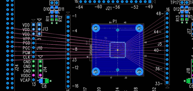
- Placement of critical parts.
- Do you have a specific part placement for some items like connectors, LEDs, power ports, USB connectors, etc.?
- These parts will be placed first.
- Next the rest of the parts will be placed in such a way to make the routes flow as smoothly as possible.
- This is done by looking at the flow of the rats nest. A rats nest is a bunch of nets that have not yet been connected to anything. These show the proper connection points.
- After the rats have been connected they turn into traces or planes (Power or Ground)
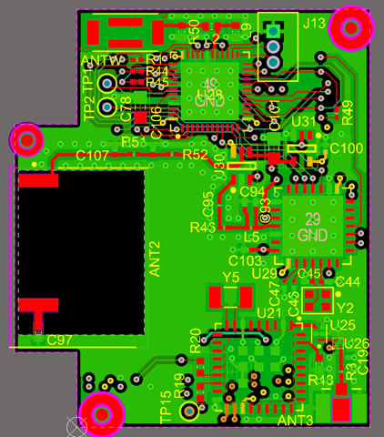
- Once the layout has been completed and the DRCs (design Rules Check) have been run and cleared the layout is ready to be finalized.
- CAM files, more commonly referred to as Gerber files are then generated.
- These are then sent to a PCB Fabricator and the design is turned into the live board.
AT BTI our layout team members are equipped with the latest in Cadence, Mentor Graphics and Altium PCB layout packages.
We specialize in all forms of PCB Layout which include:
- Surface Mount, Through-hole, Mixed Technology, BGAs and QFNs.
- Multi-Layer, Single-Layer, Double-Sided, Blind and Buried Vias.
- Fine line, Curved Traces, Teardrop Pad Generation, Copper Pour and Split / Mixed Planes.
- High-Speed, Matched Impedance and Differential Pairs.
- Analog, Digital, High Voltage and High Current.
- Gate Swap, Pin Swap, Forward and Back ECOs.
- Rename Reference Designators and Back Annotate Schematics.
- Comprehensive checklists, Layout Guidelines and DRCs.
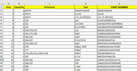
- Schematic Capture and BOM generation.
BTI maintains an extensive library of standard components and has developed a unique naming convention that is easy to follow and understand. Libraries contain the part designator, manufacturer data, specific attributes and PCB decal, which makes specific or custom BOMs easy to generate.
Get a Quote Today: Learn More